Area Selective Ald

Area Selective Atomic Layer Deposition Conformal Coating
www.semanticscholar.org

Cmos Compatible Strategy Based On Selective Atomic Layer
iopscience.iop.org

Less Is More Enhancement Of Photocatalytic Activity Of G C3n4
www.sciencedirect.com
Https Research Tue Nl Files 99950918 20180705 Co Mameli Pdf

Controlled Synthesis Of Pd Pt Core Shell Nanoparticles Using Area
www.nature.com
Three Dimensional Area Selective Atomic Layer Deposition
studylib.net
On the basis of this title there are already a few comments to make.

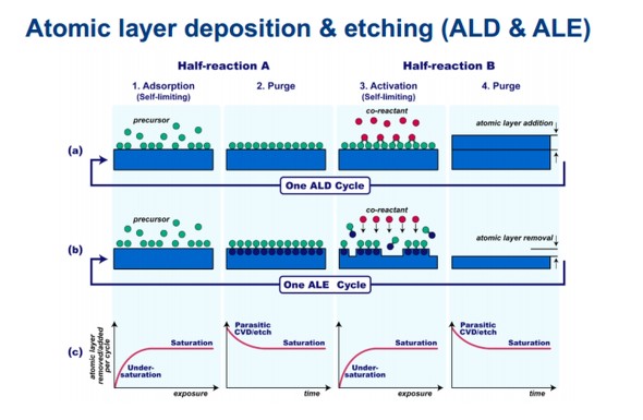
Area selective ald. First of all it dealt with ald as most of the presentations during the workshop. Tutorial on area selective atomic layer deposition stacey f. 1605 1620 area selective ru ald for sub 7 nm bottom up metal interconnects ivan zyulkov ku leuven imec 1620 1635 area selective deposition of metal films john g.
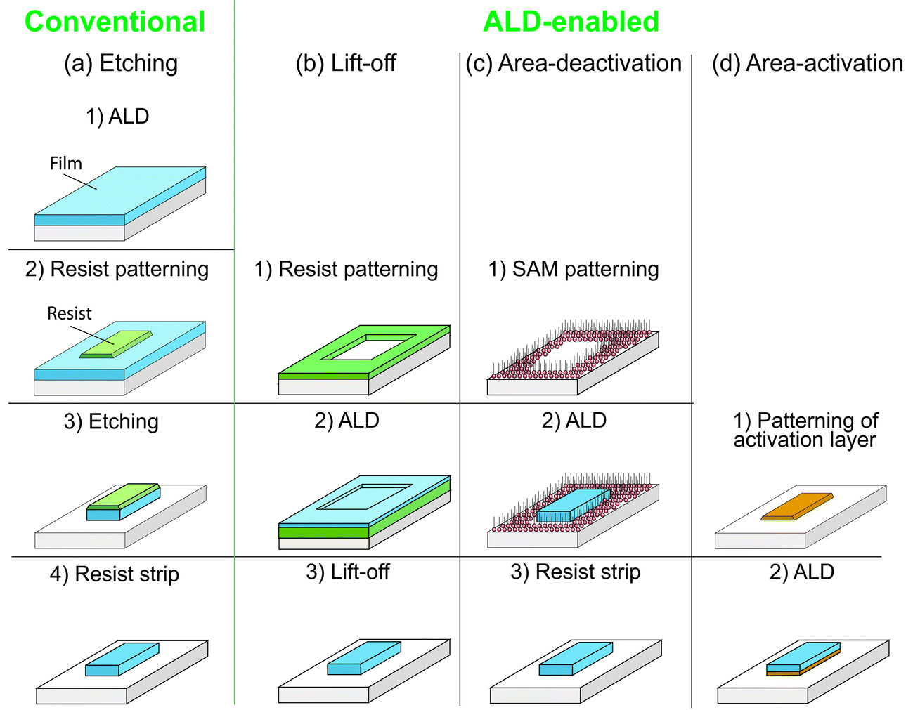
Among many competing techniques area selective atomic layer deposition as ald is a promising method that is well suited to the requirements without the use of complicated complementary metal oxide semiconductor cmos incompatible processes. In a sense area selective ald utilizes effects that historically have annoyed ald users namely that due to the chemical nature of ald nucleation can depend on the initial surface. Area selective ald by area activation.
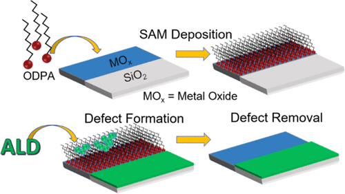
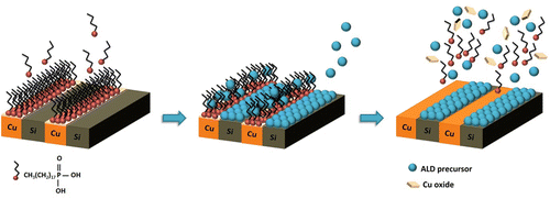
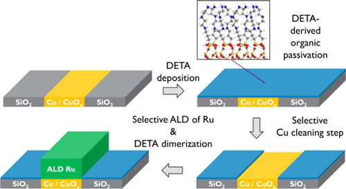
Both area selective atomic layer deposition ald and area selective molecular layer deposition mld are demonstrated on cusio 2 patterns using octadecylphos phonic acid odpa self assembled monolayers as a resist layer. In this work the dmadms and dmatms si precursors are utilized as inhibitors for area selective ald as ald. The title of my presentation of last year was ald enabled nanopatterning.
X ray photoelectron spectroscopy and auger electron spectroscopy conrm that during a metal oxide ald process. The inhibitors selectively adsorb on a sio2 surface but not on hsi so that. Most notably the semiconductor industry has relentlessly pursued sub 10 nm transistor fabrication for next generation devices an endeavor that increasingly relies on selective deposition techniques to.
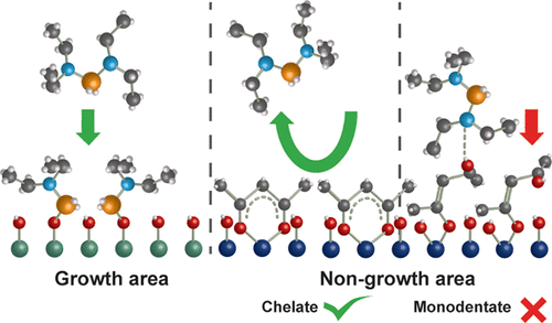
The main challenge is to understand and control thin film nucleation. 67 this review paper was published just before the recent surge of interest in area selective deposition caused by the imminent need for self aligned fabrication in semiconductor processing. Short chain aminosilanes namely bisnn dimethylaminodimethylsilane dmadms and nn dimethylaminotrimethylsilane dmatms have been used as si precursors for atomic layer deposition ald of sio2.
The difference is you trick the ald process so that it grows on material a but does not grow on material b. Ekerdt universtiy of texas at austin 1635 1655 selective deposition. Area selective deposition also uses ald but its different than traditional ald.
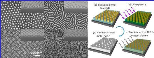
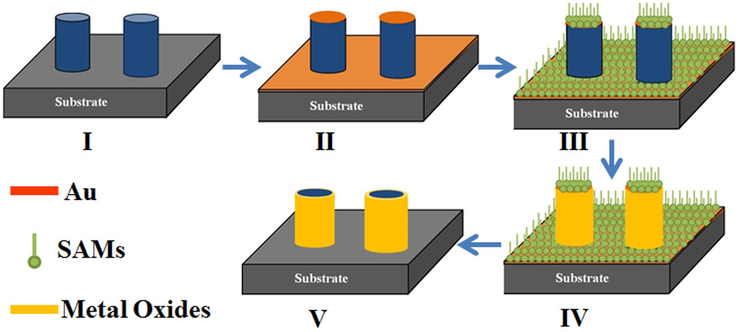
Area selective ald here in the configuration of direct write ald can be used to pattern electrical contacts on sensitive nanomaterials such as carbon nanotubes or graphene. Developments in nanoelectronics and nanoscale surface modification have continued to drive the need for more elegant and reliable bottom up area selective deposition asd strategies.

Area Selective Atomic Layer Deposition Of Titanium Dioxide
smartech.gatech.edu
Integrated Isothermal Atomic Layer Deposition Atomic Layer Etching
www.x-mol.com

A Top Surface Imaging Method Using Area Selective Ald On
smartech.gatech.edu

Area Selective Atomic Layer Deposition Of Ru On Electron Beam
www.researchgate.net
Bald Engineering Born In Finland Born To Ald 15 Nm Resolved
www.blog.baldengineering.com
Https Pubs Acs Org Doi Pdf 10 1021 Acsnano 7b04701
Https Is Muni Cz El 1431 Podzim2017 Fb041 Um Ald Tutorials Ald2017 Tutorial2 Mackus Area Selective Ald Handhouts Pdf
prezi.com

Area Selective Atomic Layer Deposition Of Noble Metals
chemrxiv.org

From The Bottom Up Toward Area Selective Atomic Layer Deposition
europepmc.org

From The Bottom Up Toward Area Selective Atomic Layer Deposition
europepmc.org
Bsa 14 03 Patterning By Area Selective Oxidation
www.bnl.gov

Transport Behavior Of Atomic Layer Deposition Precursors Through
smartech.gatech.edu

Area Selective Ald Youtube
m.youtube.com
Https Pubs Acs Org Doi Pdf 10 1021 Acs Chemmater 8b00017

Towards Area Selective Atomic Layer Deposition With High
www.atomiclimits.com

Paper Reaction Mechanism Of Area Selective Atomic Layer
hbrleelab.blogspot.com

Towards Area Selective Atomic Layer Deposition With High
www.atomiclimits.com

Fully Self Aligned Vias The Killer Application For Area Selective
www.atomiclimits.com
Area Selective Atomic Layer Deposition Assisted By Self Assembled
www.x-mol.com
C En On Twitter Area Selective Atomic Layer Deposition Ald
twitter.com

From The Bottom Up Toward Area Selective Atomic Layer Deposition
europepmc.org

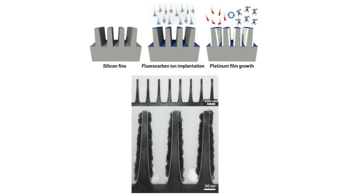
Selective Growth Of Platinum Nanolines By Helium Ion Beam Induced
www.sciencedirect.com

Sequential Regeneration Of Self Assembled Monolayers For Highly
onlinelibrary.wiley.com

Fully Self Aligned Vias The Killer Application For Area Selective
www.atomiclimits.com
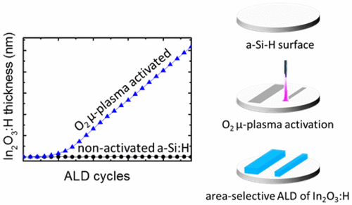
Area Selective Atomic Layer Deposition Of In2o3 H Using A M Plasma
www.x-mol.com
Https Avs Scitation Org Doi Pdf 10 1116 1 5049361 40jva 2019 Ald2019 Issue 1

Approaches To Realize Area Selective Ald A C And E And
www.researchgate.net

Vacuum Ultraviolet Photochemical Selective Area Atomic Layer
cyberleninka.org

Bald Engineering Born In Finland Born To Ald Rapid And
www.blog.baldengineering.com

Jvst A Jvst B On Twitter Jvsta Editor S Pick Vapor Deposited
twitter.com

Where Is Selective Deposition
semiengineering.com

Bottom Up Nanopatterning By Selective Atomic Layer Deposition Cocoon
www.cocoon.ugent.be

Coating Strategies For Atomic Layer Deposition In Nanotechnology
www.degruyter.com
2
Https Iopscience Iop Org Article 10 7567 1347 4065 Ab4754 Pdf
Https Ieeexplore Ieee Org Iel7 8366960 8403797 08403864 Pdf
Https Ieeexplore Ieee Org Iel7 8366960 8403797 08403864 Pdf

Tech Brief A Look At Atomic Layer Deposition Ald Lam Research
blog.lamresearch.com

Figure 1 From Area Selective Atomic Layer Deposition Of In2o3 H
www.semanticscholar.org

Ald Overcoating Strategies To Build The Metal Oxide Interface A
www.researchgate.net

Selective Atomic Layer Deposition Ald Scheme Developed In This
www.researchgate.net

Pdf Blocking The Lateral Film Growth At The Nanoscale In Area
www.academia.edu

Where Is Selective Deposition
semiengineering.com

Where Is Selective Deposition
semiengineering.com
Http Citeseerx Ist Psu Edu Viewdoc Download Doi 10 1 1 875 428 Rep Rep1 Type Pdf

The Use Of Atomic Layer Deposition In Advanced Nanopatterning
pubs.rsc.org

Delft University Of Technology Product And Process Engineering
cheme.nl

Chemistry For Positive Pattern Transfer Using Area Selective
onlinelibrary.wiley.com
Area Selective Atomic Layer Deposition Conformal Coating
www.x-mol.com

Catalysis Connected Utrecht Slides Of Invited Talk By Prof Riikka
www.slideshare.net
Ald Academy On Nucleation And Area Selective Deposition Ald Academy
www.aldacademy.com

Achieving Area Selective Atomic Layer Deposition On Patterned
aip.scitation.org

New Developments In Area Selective Deposition Take Home Messages
www.atomiclimits.com
Self Correcting Process For High Quality Patterning By Atomic
www.x-mol.com
Https Ieeexplore Ieee Org Iel7 8366960 8403797 08403864 Pdf

Atomic Layer Deposition On Self Assembled Monolayers Intechopen
www.intechopen.com

Nanopatterning By Direct Write Atomic Layer Deposition Nanoscale
pubs.rsc.org
Https Www Asd2019 Workshop Org Images Asd19 Book Of Abstracts Pdf

Where Is Selective Deposition
semiengineering.com

Area Selective Atomic Layer Deposition Of Sio2 Using Acetylacetone
www.semanticscholar.org

Tu E Energy Annual Research Report 2015 By Tu E Strategic Area
issuu.com
Area Selective Atomic Layer Deposition Of In2o3 H Using A M Plasma
docksci.com
eetimes.jp

The Use Of Atomic Layer Deposition In Advanced Nanopatterning
pubs.rsc.org
Https Www Asd2019 Workshop Org Images Presentations Biyikli Asd 2019 Pdf
The Use Of Atomic Layer Deposition In Advanced Nanopatterning
pubs.rsc.org

Nanomanufacturing Ald Fundamentals
www.nanomanufacturing.nl
Area Selective Ald Of Ru On Nanometer Scale Cu Lines Through
www.x-mol.com

Approaches And Opportunities For Area Selective Atomic Layer
www.semanticscholar.org
Https Avs Scitation Org Doi Pdf 10 1116 1 5000587
Mechanism Of Precursor Blocking By Acetylacetone Inhibitor
www.x-mol.com

Atomic Layer Deposition On Self Assembled Monolayers Intechopen
www.intechopen.com
Https Www Mdpi Com 2076 3417 9 10 1990 Pdf

Coating Strategies For Atomic Layer Deposition In Nanotechnology
www.degruyter.com

Bald Engineering Born In Finland Born To Ald The Website For
www.blog.baldengineering.com

Towards Area Selective Atomic Layer Deposition With High
www.atomiclimits.com

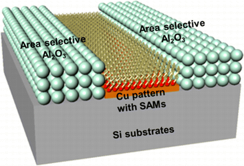
Visualization Of Cvd Grown Graphene On Cu Film Using Area
www.sciencedirect.com

From The Bottom Up Toward Area Selective Atomic Layer Deposition
europepmc.org

New Developments In Area Selective Deposition Take Home Messages
www.atomiclimits.com

Principle Of Area Selective Ald Showing Growth On Certain Surface
www.researchgate.net
Https Research Tue Nl Files 99950918 20180705 Co Mameli Pdf

Approaches To Realize Area Selective Ald A C And E And
www.researchgate.net

Atomic Layer Deposition System Ppt Video Online Download
slideplayer.com
Https Pubs Acs Org Doi Pdf 10 1021 Acs Chemmater 8b03454

Area Selective Atomic Layer Deposition Of Sio2 Using Acetylacetone
www.semanticscholar.org

Area Selective Atomic Layer Deposition Of Noble Metals
chemrxiv.org
Https Pubs Acs Org Doi Pdf 10 1021 Acs Chemmater 8b03165

Bald Engineering Born In Finland Born To Ald Area Selective
www.blog.baldengineering.com
Fesem And Fib Used In Area Selective Atomic Layer Deposition
blogs.mtu.edu
Application Of Three Dimensionally Area Selective Atomic Layer
www.nature.com

New Developments In Area Selective Deposition Take Home Messages
www.atomiclimits.com

Area Selective Ald Youtube
www.youtube.com

Self Focusing Sims A Metrology Solution To Area Selective
www.sciencedirect.com